Login / Register
Micron Technology does more than talk about artificial intelligence (AI). Using data analytics and AI in its own manufacturing processes, the company literally puts its money where its mouth is, demonstrating the value to businesses of the technologies Micron enables with its next-generation memory and storage solutions. The benefits are many, including higher yields, a safer working environment, improved efficiencies and a sustainable business.
The enterprise’s factories produce memory technologies on silicon wafers through a highly complex and precise process. The potential for error and for waste is high. But data and AI are helping to reduce that potential. When relying on human vigilance to spot and track flaws, mechanical problems and other trouble areas, the organization lost time and money — losses that can be avoided with today’s sophisticated technologies.
Linus Sebastian of Linus Tech Tips visits a Micron R&D fab and explains some of the complexities of semiconductor manufacturing.
Complex manufacturing process
Silicon manufacturing is an extremely complex process, taking months and involving some 1,500 steps. Micron employs sophisticated AI throughout the process to improve accuracy and coverage.
“We have built something here that is completely differentiated,” explains Koen de Backer, Micron vice president of smart manufacturing and artificial intelligence. “We’re seeing much, much higher levels of accuracy. We can now launch products twice as fast — while improving productivity by 10%. It’s truly been transformative. You could say it’s a killer app.”
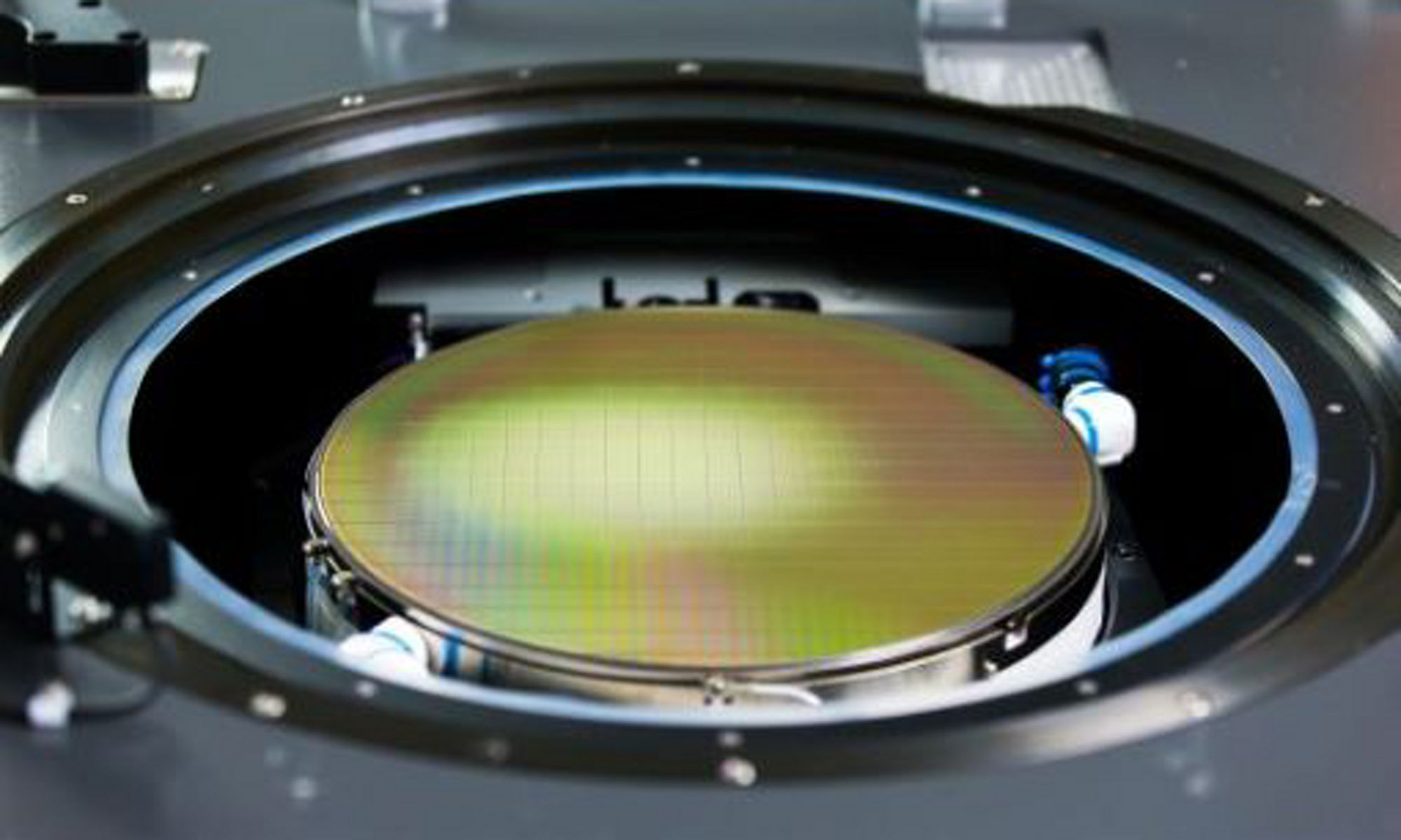
Wafer creation
The process starts with silicon. Wafers, used as the foundation for computer chips, are made from silica, a type of sand, which must be filtered and refined to 99.999% purity. This electronic-grade silicon is melted and compressed into ingots, which are sliced into extremely thin — 0.67mm thick — wafers.
The wafers are polished to remove any marks from the cutting, coated with a thin layer of photo resistant material, and etched with the design of the circuitry they will be supporting using a process similar to photography. The more complicated the circuitry, the more images are imprinted onto the wafer. This process happens layer by layer, with each layer treated separately and either blasted with ionized plasma, a process known as “doping,” or bathed in metals. The finished wafer is then coated with a thin protective film before being tested to ensure that it works as intended.

The manufacturing process takes place in sterile fabrication rooms (called cleanrooms) designed to prevent even the tiniest speck of dust from falling on the pristine wafers. But damage does occur. The fragile wafers may get scratched, nicked or punctured, or bubbles may form under the protective film.
Often, these flaws are microscopic — completely invisible to the naked eye. Even when they are visible, people scanning the 30 to 40 photos captured of each wafer during the photographic imaging process can overlook defects due to eye fatigue or momentary inattention. Blink, and they’ve missed the flaws.
When problems aren’t caught until the test phase, a lot of time and money has already been wasted. Chances are the issue causing the flaw affects more than one wafer — possibly even thousands.
Other things can go wrong in production as well. Parts wear out; pipes leak or drip hazardous chemicals onto products or people. Catching and correcting these issues early is imperative. Shutdowns are very expensive, leading to loss of revenue and missed productivity time. And given the complexities of semiconductor manufacturing, the many hours spent in recovery could put the true cost in the millions. What’s more, the risks associated with worker injuries are numerous. Finally, Micron’s commitment to sustainability demands that the process become as energy efficient as possible.
Detecting problems in products and machinery is vital for manufacturing efficiency, effectiveness and safety. Unfortunately, to err is human, and even the most highly trained person will not always see, hear or feel the very minute and subtle indicators that something is awry.
Artificial intelligence technologies, however, can perform these tasks with laser-sharp precision and in a fraction of the time. Micron collects petabytes of manufacturing data from more than 570,000 sources which is added to Micron’s cloud data base environments.
Image analytics
The foundation of Micron’s AI-enabled manufacturing is image analytics. “Images are quite powerful in semiconductor manufacturing process,” explains Koen, “You can analyze detailed images of each step of the process.”
“By analyzing every stage,” he continues, “we can quickly identify any kind of deviation that happens — all in a completely automated way. This analysis spans everything – front end, assembly and test.”
In addition to images, Micron similarly employs video analytics to eliminate quality issues in assembly and testing. You may think video would be too data-intense to be practical. Yet, Micron again uses AI to identify the critical places to analyze. AI starts and stops the video stream to only capture the critical processes, keeping data size in check.
Imaging and video are especially effective, as wafer flaws come in many forms. For the most part, they fall into one of a few common categories: tiny holes near the wafer’s edge or scratches and bubbles in the outer film. Micron’s AI systems use “computer vision” technology to spot these defects on the images the photolithographic cameras capture as they etch circuitry onto the wafers during manufacturing.
Engineers might direct the system to scan for tiny dots (holes) at the wafers’ edges, for instance, or for contiguous or slightly broken lines (scratches), or the system may seek color variations resulting in dark or light spots or patterns. Some of these flaws can be spotted in near real time, with the system sounding alerts within seconds after an image is taken. Other defects might be discovered during secondary scans minutes after the photographs are stored. All these processes rely on the AI system’s use of two million images stored in the database environment for comparison and contrast.
The results have proven far more accurate than engineers’ assessments, as AI computer vision has higher accuracy and high efficiency. Best of all, engineers can now focus on the problem — and on data collection.
And with Micron’s AI automatic defect classification (ADC) system, technicians and engineers no longer need to classify wafer defects manually. Instead, AI-ADC uses deep learning to sort and categorize millions of flaws every year. Micron created this system using the latest imaging techniques available today, including neural networks, described as a biologically inspired programming paradigm that enables a computer to learn from observational data.
This form of machine learning categorizes images according to their flaws, placing them in discrete clusters. Not only does this process help engineers to discover what went wrong during manufacturing for an early fix that avoids more defects, but it also enables AI systems to find flaws on their own and refine results with each iteration.
Acoustic listening
While AI imaging is at the core of the manufacturing process, Micron also employs acoustic listening to preempt issues. Often, “abnormal” sounds signify a wearing part or imminent breakdown.
Micron’s AI systems are listening for anomalies in our factory machinery via audial sensors installed strategically near robotic actuators or close to pumps. These microphones record normal activity for several weeks, and software converts the detected frequencies into graphs or charts depicting the sounds as visual data. When a new pitch or frequency appears, the system issues an alert. Often, it can even discern the cause of the anomaly.
Searching these massive databases can be time consuming. When a machine is in danger of a breakdown, however, plant managers need to know in the instant. Sending the data to an AI system filled with GPU’s, accelerators, and importantly Micron memory and storage to provide fast, intelligent results much more quickly than CPU-based systems can. All these AI systems with hundreds of thousands of GPU cores and memory working simultaneously and synergistically can refine their results in the blink of an eye with little or no human intervention. Plus, they can improve their diagnostics with each iteration, similar to how the human brain works.
Thermal imaging
Not every malfunction makes noise — and in a manufacturing environment, silence can be deadly. In many instances, the temperature changes instead. Until recently, the only way to detect a surge in temperature was to see a red glow, sparks or smoke. By the time these appeared, the problem had already entered the danger zone, and the plant needed to evacuate workers.
So, in addition to image analytics and acoustic listening, Micron also uses thermal imaging, which measures the temperature of key components.
“Temperature measurement on transformers is key to prevention of overheating,” Koen explains, “Early detection can make the difference between doing a simple repair and replacing an entire, expensive piece of equipment.”
Finally, these AI sensors for imagery, sound and temperature deliver on Micron’s commitment to sustainability. “These sensors excel for quality and efficiency improvements, but also for sustainability,” Koen adds. “They deliver granular metering of energy, leading to significant usage and energy savings.”
The numbers
At Micron, 570,000 sensors produce 2.3 million wafer images in 229 million control points. All are run through AI models each week. In addition, 34 petabytes of data are stored, and 30 terabytes of new data are captured each day.
This AI adoption at scale analyzes innovative data science applications in yield analytics, digital-twin planning, IoT and image analytics, optimization and advanced algorithms, process automation and mobile applications.
The results* are undeniable:
- 4% improvement in manufacturing tool availability
- 18% improvement in labor productivity
- 50% reduction in time to market for new products
- 22% reduction in product scrap
- 50% faster time to resolve quality issues
* Improvements based on Micron internal data and analysis gathered from 2016 through 2020
And the benefits of data analytics and AI extend beyond the fab to every aspect of Micron’s operations: sales and marketing, human resources, business operations, research and development, and more.
“This is about transforming the enterprise, not just the shop floor,” Koen says. “We can bring these techniques and methods to all the business processes within the company.”
Ecosystem partnerships
Beyond optimizing the internal manufacturing process, Micron also works directly with suppliers, giving them detailed feedback on their products to ensure the best energy efficiency. With these suppliers, Micron coordinates DIMS (data ingestion into Micron systems) so that ingestion happens at the highest frequencies. Micron engineers monitor this ingestion in real time. Likewise, correction and optimization are constantly taking place at extremely granular levels.
In addition, working with our suppliers, Micron uses telemetry data to measure the effect of our products in their data centers. This data, combined with internal data, underpins real-time collaboration to improve products for their specific workloads.
We also closely monitor the performance of our models. Using AI on incoming data and retraining allows engineers to focus at a higher level on automating the machine learning flow. (Otherwise, there would never be enough data scientists to keep up, and they’d be chasing events that already happened.)
These initiatives are backed by an internal data science academy and continued investment in in-house data scientists, engineers and solution architects. These resources, along with our citizen data science model, enable functional experts to use Al-powered tools and insights.
Industry leadership
Today, Micron combines a rich heritage of core process knowledge with the unparalleled efficiencies of AI. Data experts have created large yield management platforms used by 6,000 people across the company. At the same time, dedicated teams focused on day-to-day yield optimization are building new prototypes in fast integration cycles. These prototypes are frequently implemented to optimize the major platforms.
Meanwhile, the results speak for themselves. The dedication of Micron team members and AI-powered manufacturing processes enabled our 1α (1-alpha) node DRAM and 176-layer NAND to hit the highest yields in Micron’s history. And the industry-leading 1β (1-beta) DRAM and 232-layer NAND achieved mature yields faster than any other Micron technology.
Micron is optimizing how AI transforms manufacturing. Far from taking everyone’s jobs, this new technology is augmenting and empowering teams who no longer focus on acquiring data and doing multiple base analyses. Now they can focus on what they’re good at — innovating to develop industry-leading products.